


China's Wafer Fab Equipment Industry Present & Future
Covering the present tools & future roadmap of NAURA, AMEC, ACM Research, SiCarrier and Piotech


The advent of LLMs and the intensification of the US-China rivalry have placed semiconductors at the undisputed center of global power dynamics. While headlines frequently focus on the progress of Chinese chip designers like Huawei and foundries such as SMIC and CXMT, a critical yet far more opaque segment of the supply chain remains largely in the shadows: the domestic Wafer Fab Equipment (WFE) sector. It is these complex machines that will ultimately determine the success or failure of Beijing’s chip ambitions. Historically reliant on foreign technology, China is now driven by a national mandate for self-sufficiency and is pouring immense resources into cultivating its own domestic WFE ecosystem.
Key Chinese semiconductor equipment manufacturers AMEC, Naura, ACM Research, Piotech, and SiCarrier are rapidly advancing their product roadmaps and launching new etching, deposition, cleaning, and metrology tools. Their main focus is on achieving greater technological self-sufficiency, expanding into advanced process nodes, and increasing global competitiveness. They still face significant challenges in matching the breadth and depth of established global leaders. Their strategies involve significant investment in research and development, and aggressive expansion of product portfolios. While they have made notable progress in areas like etching, deposition, and cleaning, they continue to face intense competition from established global giants who dominate the market.
AMEC (Advanced Micro-Fabrication Equipment Inc. China)

Founding & Early Years
AMEC was founded on May 31, 2004, by Dr. Gerald Yin, who previously held senior management positions at Applied Materials. The company started with a vision to become a leading global supplier of high-end semiconductor processing equipment. A significant early milestone was the development of China’s first domestically produced dielectric etch system. This achievement marked a crucial step in China’s efforts to build a self-reliant semiconductor equipment industry. In its initial years, AMEC focused on developing and refining its core etching technologies. By 2007, the company had successfully developed and shipped its first etching and thin film equipment to a domestic customer. Strategic financing rounds, including a $38 million Series A funding in 2005 and a $58 million Series C funding in 2008, enabled it to accelerate R&D and market entry. By 2008, AMEC had several of its Primo Etch™ dielectric plasma etching systems and Primo HPCVD™ systems undergoing trials at major Asian chip manufacturing plants.
A key turning point was the resolution of intellectual property disputes with Applied Materials around 2010, which allowed AMEC to focus on its growth trajectory. The company’s Primo D-RIE™ (Dual Frequency Reactive Ion Etch) system, launched in the late 2000s, gained significant traction for its innovative design, high productivity, and cost-effectiveness, winning industry awards and being adopted by numerous customers for 65/45/32nm and more advanced chip manufacturing. A major corporate milestone was its listing on the Shanghai Stock Exchange’s STAR Market in July 2019. Over the years, AMEC has grown from a small startup to a global enterprise with over 2,000 employees and more than 5,000 reaction chambers installed and running in over 130 production lines worldwide by 2024.
The company has rapidly grown to become a key player in the global semiconductor equipment industry, particularly recognized for its advancements in plasma etching and Metal Organic Chemical Vapor Deposition (MOCVD) technologies. AMEC’s mission is to provide leading-edge processing equipment and process technology solutions to global integrated circuit (IC) and LED chip manufacturers, thereby assisting clients in enhancing their technological capabilities, boosting productivity, and reducing manufacturing costs. The company’s strategic focus revolves around organic growth through intensive research and development, complemented by selective investments and collaborations, rather than relying heavily on mergers and acquisitions. AMEC has strategically expanded its operations beyond mainland China to establish a significant global footprint. The company’s headquarters are located in Shanghai, China, which serves as its primary hub for research, development, and manufacturing. To support its global customer base, AMEC has established regional subsidiaries and service centers in key international locations. These include AMEC Japan Co., Inc. in Japan, AMEC North America, Inc. in the United States, and Advanced Micro-Fabrication Equipment Korea Ltd. in South Korea. Additionally, the company operates Advanced Micro-Fabrication Equipment International Pte. Ltd. in Singapore, which handles trade sales. This network of international subsidiaries enables AMEC to provide comprehensive, seamless support to its customers worldwide, covering aspects from system preparation and start-up to process integration, sign-off, warranty, and post-warranty services.
AMEC’s leadership has articulated a clear vision for the future, targeting an expansion of their product coverage from the current 30% to 60% of high-end integrated circuit equipment within the next five to ten years. This ambitious goal encompasses not only their core strengths in etching and thin-film deposition but also extends to metrology and inspection tools, as well as certain wet processing equipment, positioning AMEC as an emerging platform-based equipment provider. The company is also reportedly exploring pathways to achieve 5nm process nodes without relying on EUV (Extreme Ultraviolet) lithography, with the help of their ultra-precise etching tools.
In 2022, AMEC reported a total revenue of approximately 4.74 billion RMB. This figure saw a substantial increase in 2023, reaching 6.26 billion RMB. The growth momentum continued into 2024, with the company achieving a remarkable revenue of approximately 9.07 billion RMB. This represents a year-over-year growth of approximately 44.73% from 2023 to 2024. The primary driver for this revenue surge in 2024 was the significant increase in sales of its etching equipment, which contributed approximately 7.28 billion RMB, marking a 54.72% increase compared to the previous year. While MOCVD equipment sales experienced a slight decline of about 18.03% to 379 million RMB in 2024, the company successfully introduced its LPCVD equipment to the market, generating sales of approximately 156 million RMB in its first year.

A cornerstone of AMEC’s strategy is the aggressive development of thin-film deposition equipment, which is projected to grow significantly, potentially reaching half the scale of their established etching equipment business within three to five years. This expansion is critical as thin-film processes are integral to advanced semiconductor manufacturing, especially with the transition to 3D device architectures and sub-10nm technology nodes, where the complexity and number of deposition steps are increasing. The company is actively working on approximately 40 different types of thin-film deposition equipment, with a notable emphasis on addressing market gaps created by international export restrictions. Specifically, AMEC plans to complete the development of over 20 types of such embargoed thin film equipment to cover all advanced metal applications by 2029. Recent successes in this area include the rapid market adoption of their LPCVD (Low-Pressure Chemical Vapor Deposition) and ALD (Atomic Layer Deposition) tungsten metal deposition systems. For instance, after shipping only one unit in 2023, AMEC delivered 128 units in 2024, with expectations of further substantial growth in 2025. This rapid scaling underscores both the market demand and AMEC’s manufacturing and support capabilities. The company’s LPCVD and ALD equipment, particularly for metal tungsten applications, have seen rapid market adoption, with LPCVD equipment shipments exceeding 150 reaction chambers within a year of market validation and securing substantial orders (approximately 476 million RMB in 2024).
Etching
The company has developed three generations and 18 models of etching machines over the past two decades, with an accelerating pace of product development. Nearly 4,000 Capacitively Coupled Plasma (CCP) etching reaction chambers are operating in logic production lines globally. As of 2024, AMEC had over 270 CCP etching reaction chambers operating in 5nm and below production lines globally. In 2024 alone, over 1,200 CCP etching reaction chambers were produced and shipped. The company is also heavily investing in its ICP etching technology, with the Nanova LUX series (Nanova LUX-WT, Nanova LUX-Cryo) already in production or customer validation, and the next-generation Primo Nanova 2G under development in the lab. These ICP etchers are crucial for applications in advanced logic, power devices, Micro-LEDs, and specialized structures like metalenses for AR/VR. A key technological differentiator for AMEC is its “dual reaction chamber” design, which offers high throughput and lower processing costs while maintaining exceptional precision. The ICP dual-chamber system, Primo Twin-Star®, achieves an etching precision of 0.2 Å/min (0.02 nm), equivalent to one-tenth the diameter of a silicon atom, and has shown minimal deviation between chambers in rigorous testing. This level of precision is critical for advanced nodes. Furthermore, AMEC is developing specialized etching solutions for challenging applications, such as ultra-high aspect ratio (UHAR) etching for 3D NAND and DRAM manufacturing. Their UHAR CCP etchers, designed for aspect ratios of 60:1 or higher, and UHAR ICP etchers for mask etching at aspect ratios of 40:1 or higher, have been successfully verified and are entering mass production. The company is also reportedly developing even more advanced 90:1 high aspect ratio etchers, which could contribute to revenue from late 2025 or 2026 (YMTC 3D NAND). Recent product launches include the Primo Twin-Star, an etching system with sub-angstrom precision (0.2Å), and the Primo Halona, a 12-inch wafer edge etching device, both designed for 5nm and below processes

Beyond core etching and thin-film deposition, AMEC is strategically expanding into other critical equipment segments. The company has been investing in metrology and inspection, particularly electron beam inspection, for seven to eight years, recognizing its importance for advanced process development and as a domestic shortcoming. Instead of acquiring existing players, AMEC has chosen to build its own team with top global experts. This aligns with their philosophy of building core technological expertise internally. The company’s R&D efforts are extensive, with over 20 new equipment types across six major categories currently in development. These include next-generation CCP and ICP etchers, bevel etchers, LPCVD and ALD film equipment, silicon and silicon-germanium epitaxial (EPI) growth systems, PECVD (Plasma-Enhanced Chemical Vapor Deposition) equipment with new plasma sources, and the aforementioned electron beam inspection tools. Newly developed silicon/germanium-silicon EPI and bevel etching equipment are also slated for market verification in the near term. This broad R&D portfolio indicates a clear roadmap towards becoming a more comprehensive equipment supplier.
MOCVD
AMEC’s MOCVD equipment, particularly for gallium nitride (GaN)-based LED production, has already achieved global leadership, holding over 80% of the market share for GaN-based LED lighting equipment. In the MOCVD market, AMEC’s Prismo series, particularly the Prismo A7™, has established a dominant position. The company celebrated the shipment of its 100th Prismo A7 reaction chamber in May 2025. The company continues to innovate in this space, with the Prismo UniMax® MOCVD system for Mini-LED applications gaining significant traction since its launch in June 2021, recognized for its high yield, uniformity, and throughput. The Prismo HiT3 for deep UV LEDs and Prismo PD5 for GaN power devices have also secured repeat orders from clients, indicating successful market entry and validation. AMEC is also actively developing MOCVD solutions for emerging applications. This includes equipment for silicon carbide (SiC) power devices (currently in production verification), GaN Micro-LED blue/green light equipment( approved and entered production), and GaN power device epitaxy equipment, along with gallium arsenide (GaAs) red/yellow light equipment both expected to enter production within the year. Furthermore, MOCVD equipment for Micro-LED high-end displays is progressing well, with laboratory results showing excellent wavelength uniformity. A prototype has been shipped to a leading domestic customer for production verification. This diversification within the MOCVD segment highlights AMEC’s strategy to leverage its core technology across multiple high-growth areas in the compound semiconductor and display markets.

The company’s commitment to R&D is substantial, with investment increasing by 94.3% in 2024 to reach RMB 2.45 billion, accounting for approximately 27% of its revenue, a notable rise from 20.15% in 2023 and 19.59% in 2022. The 94.13% year-on-year increase in R&D spending in 2024 compared to 2023 further highlights this aggressive ramp-up. This high level of investment has significantly shortened new product development cycles from 3-5 years to about two years or even less. To support this growth and expansion, AMEC is also scaling its manufacturing infrastructure, with new production and R&D bases, such as the one in Lingang, Shanghai, significantly increasing its operational footprint. A new R&D and production base in Chengdu, with an investment of approximately 3.05 billion RMB, is planned for the 2025-2030 period, focusing on CVD & ALD, E-Beam inspection tool, and other critical equipment for advanced logic and memory chips. The company is focused on achieving even higher precision, better critical dimension control, and improved selectivity for complex 3D device architectures like Gate-All-Around (GAA) transistors and increasingly dense 3D NAND structures. The development of the Primo Nanova 2G ICP etcher is a step in this direction, aiming to provide enhanced capabilities for advanced logic and specialty device manufacturing. They have 2,941 patent applications filed by March 2025, 83% of which are invention patents. AMEC plans to apply for at least 300 patents globally in 2025. The company’s long-term vision extends to 2035, by which it aims to become a globally first-tier semiconductor equipment company in terms of scale, product portfolio, competitiveness, and customer satisfaction. As AMEC continues to innovate and expand its product portfolio, it is likely to capture a larger share of the global WFE market, particularly in its core strengths of etching and MOCVD, and increasingly in deposition.
Naura Technology Group Co., Ltd.

NAURA Technology Group Co., Ltd., originally founded as Beijing Sevenstar Electronics Co., Ltd., has a rich history deeply intertwined with China’s development of its domestic electronics and semiconductor industries. In 2001, a significant milestone was reached with the establishment of two key entities: Beijing Sevenstar Electronics Co., Ltd. and Beijing North Microelectronics Co., Ltd.. Sevenstar Electronics initially focused on a range of products, including integrated circuit (IC) manufacturing equipment such as diffusion/oxidation furnaces, cleaning machines, hybrid integrated circuits, and electronic components. These products found applications across diverse fields, including ICs, solar energy, flat-panel displays, and Micro-Electro-Mechanical Systems (MEMS). Concurrently, Beijing North Microelectronics was established with a primary focus on semiconductor etching equipment, Physical Vapor Deposition (PVD) systems, and Chemical Vapor Deposition (CVD) tools, catering to the IC, advanced packaging, semiconductor lighting, and MEMS sectors. This period marked the beginning of a dedicated effort to build indigenous capabilities in semiconductor equipment, a field historically dominated by international players.
The early 2000s saw these nascent companies begin to make their mark. For instance, in 2001, North Microelectronics undertook the significant responsibility of leading a national “863 Program” project focused on plasma etching machines. This project underscored the strategic importance placed on developing domestic etching technology, a critical process in semiconductor manufacturing. The efforts of Sevenstar Electronics and North Microelectronics were pivotal during a time when China was starting to recognize the necessity of reducing its reliance on imported semiconductor equipment. The development trajectory of these companies was also influenced by broader industry trends, such as the transfer of industries like LED and new energy, which provided opportunities for domestic equipment manufacturers to gain traction and achieve technological breakthroughs. The establishment of these entities laid the groundwork for what would eventually become a major force in China’s semiconductor equipment landscape, setting the stage for future consolidation and growth. The initial focus on a variety of equipment types, from furnaces and cleaners to more complex etching and deposition systems, reflected a comprehensive approach to addressing the diverse needs of the burgeoning Chinese semiconductor industry.
The evolution of NAURA Technology Group is characterized by strategic mergers, acquisitions, and consistent technological advancements, transforming it into a comprehensive semiconductor equipment provider. A pivotal moment in the company’s history occurred in 2010 when Sevenstar Electronics was listed on the Shenzhen Stock Exchange, providing a platform for future growth and investment. However, the most significant transformation took place in 2016, under the guidance of the Beijing Municipal State-owned Assets Supervision and Administration Commission (SASAC). This year marked the strategic merger and reorganization of Sevenstar Electronics and North Microelectronics, leading to the formation of NAURA Microelectronics Equipment Co., Ltd. and the introduction of the new “NAURA” brand. This consolidation was a landmark event, creating a “platform-type” enterprise in the domestic semiconductor equipment sector with enhanced capabilities and a broader product portfolio. The newly formed entity, with Beijing Electronic Holding Co., Ltd. as its largest shareholder (holding over 40% stake, a figure that has remained stable), was poised to become a national champion in the semiconductor equipment industry.
Following the 2016-2017 reorganization, NAURA embarked on a series of strategic acquisitions to further bolster its technological prowess and expand its product offerings. In 2018, the company acquired Akrion Systems LLC, a U.S.-based company, to complement and strengthen its cleaning equipment product line. This was followed in 2020 by the acquisition of radio frequency (RF) application technology-related assets from Beiguang Technology, which significantly enhanced NAURA’s in-house capabilities in RF technology, a core component in many semiconductor manufacturing tools. More recently, in 2023, NAURA acquired Beijing Danpu, further expanding its capabilities in coating equipment. These acquisitions demonstrate a clear strategy of integrating key technologies and product lines to build a more comprehensive and competitive portfolio. The company’s growth has also been supported by national initiatives, with both the first and second phases of the National Integrated Circuit Industry Investment Fund (the “Big Fund”) holding equity in NAURA. The consistent investment in R&D, coupled with strategic M&A, has enabled NAURA to continuously introduce new products and achieve significant market penetration, particularly in the context of increasing domestic demand and the push for localization. A significant operational milestone was achieved in 2022 when the company’s annual sales revenue surpassed 10 billion RMB for the first time.
Key Technology

NAURA Technology Group offers a comprehensive and diverse portfolio of semiconductor manufacturing equipment and related solutions, positioning itself as a “platform-type” enterprise capable of serving a wide range of needs within the semiconductor industry. The company’s product offerings are broadly categorized into several core segments, primarily focusing on equipment for integrated circuit (IC) manufacturing, advanced packaging, semiconductor lighting (LED), power devices, MEMS, photovoltaic (PV) manufacturing, and flat-panel display (FPD) production. Within these segments, NAURA provides a multitude of specialized tools. Key product categories include plasma etching equipment (Etch), physical vapor deposition (PVD) systems, atomic layer deposition (ALD) systems, chemical vapor deposition (CVD) equipment, oxidation/diffusion furnaces (Furnace), wet process equipment (WET), cleaning systems, ultraviolet (UV) curing ovens, wafer handling and transfer equipment (Indexer), and gas measurement and control devices like mass flow controllers (MFCs). The company is recognized as the largest semiconductor equipment manufacturer in China. This leadership is reflected in its significant market share across various equipment segments. For instance, NAURA holds approximately 30% of the domestic market for etching equipment, 25% for thin-film deposition equipment, and over 2% for cleaning and epitaxy equipment. It commands a substantial 28% share of the domestic semiconductor equipment market.
Major Chinese semiconductor manufacturers, including SMIC, Hua Hong, and YMTC, are reportedly utilizing NAURA’s equipment for their 28nm and more advanced process nodes. The company’s comprehensive product portfolio, covering etching, deposition, cleaning, heat treatment, and now ion implantation, positions it as a key enabler of China’s semiconductor localization efforts. Analysts expect NAURA to continue benefiting from this trend, with projections indicating that China’s semiconductor equipment self-sufficiency rate could reach 50% by 2025, further solidifying NAURA’s role and market share within the country.
The company’s capabilities extend beyond just front-end IC manufacturing. NAURA also provides equipment for emerging and specialized markets. For instance, in the advanced packaging domain, the company offers solutions for processes like Through-Silicon Via (TSV) etching and metallization, as well as bumping processes. For the LED industry, NAURA supplies specialized etching and deposition equipment, including PSS (Patterned Sapphire Substrate) etchers and AlN buffer layer sputtering systems. In the rapidly growing MEMS and power semiconductor sectors, NAURA’s deep silicon etching and thin-film deposition tools have found widespread application. Furthermore, the company caters to the photovoltaic industry with a range of equipment for high-efficiency solar cell production, such as diffusion furnaces, PECVD systems, and wet etching machines.
In recent years, Naura has consistently launched new products, demonstrating its commitment to technological advancement and market expansion. For instance, in March 2019, the company introduced the Excor D630, a new silicon dioxide dry stripping equipment. More recent launches include the 12-inch photoresist stripper ACEi300 in June 2023, the NMC 508RIE dielectric etcher in August 2022, the plasma-enhanced silicon nitride ALD vertical furnace DEMAX SN302P in March 2024, and the gap-filling silicon oxide atomic layer deposition vertical furnace DEMAX SN302T. Their 12-inch HDPCVD (High-Density Plasma Chemical Vapor Deposition) equipment entered customer production lines in January 2024, and a domestically produced 12-inch dual damascene CCP etcher was released in March 2024. These introductions highlight Naura’s focus on expanding its capabilities in advanced node manufacturing and increasing the domestic supply of critical semiconductor equipment. The company has also significantly expanded its production capabilities with the completion of its Phase IV semiconductor equipment industrialization base in Beijing E-Town in the first half of 2024, representing an investment of 3.816 billion RMB and is expected to contribute 7.5 billion RMB in annual incremental revenue. This facility is designed to produce 500 units of IC equipment, 500 units of emerging semiconductor equipment, 300 units of LED equipment, and 700 units of PV equipment annually. Naura acquired a 17.9% stake in Kingsemi, a manufacturer of photolithography coating and developing equipment, and became the controlling shareholder. This acquisition is strategically important as Kingsemi is a leading domestic supplier of front-end coating and developing machines, and this move will fill a critical gap in NAURA’s product lineup, adding coating, chemical cleaning, and bonding capabilities
Etching
Naura’s etching equipment business has been a key area of growth and technological development. The company has over two decades of experience in this field, having delivered its first domestic dry etcher in 2005 and subsequently developing silicon etchers, metal etchers, and dielectric etchers. In 2023, Naura’s etching equipment revenue approached RMB 6 billion, with a cumulative shipment of over 3,500 chambers. Their technology spans ICP (Inductively Coupled Plasma), CCP (Capacitively Coupled Plasma), TSV (Through-Silicon Via), and dry stripping. They have developed advanced techniques, including an etching method for silicon-containing organic dielectric layers that uses cyclic alternating steps with different etching gases (oxygen-based and oxygen/fluorine-based) to achieve smoother morphology and minimize micro-grooves or protrusions, thereby enhancing device performance. The company’s 12-inch ICP etching machines have achieved 28nm process capability and are instrumental in 14/7nm Self-Aligned Double Patterning (SADP) and Self-Aligned Quadruple Patterning (SAQP) applications. They have successfully developed high dielectric constant (high-k) ALD equipment, which is essential for manufacturing high-performance logic and memory chips. Naura, as a major domestic supplier of ICP technology, had shipped over 3,200 ICP chambers by the end of 2023, with its 12-inch ICP etchers achieving breakthroughs at various technology nodes and being adopted by both domestic and international fabs. The CCP etchers, critical for dielectric etching, have also seen significant progress. Since focusing on dielectric etching technology in 2021 and launching its CCP dielectric etcher in 2022, Naura has mastered key technologies such as plasma control, chamber design, and high-power plasma feeding. By the end of 2023, over 100 CCP etching chambers had been shipped, serving logic, memory, and power semiconductor applications. The 12-inch CCP dielectric etcher, Accura LX, is designed for critical dielectric etching processes like AIO (dual damascene) and contact holes in logic, and can be extended to CMOS-related processes in memory, handling both Low-K and conventional dielectric materials.NAURA has also successfully developed atomic layer etching (ALE) equipment, which has undergone client verification. Additionally, Naura has made inroads in TSV etching technology, essential for 3D integration and advanced packaging. Their 12-inch TSV etcher, launched in 2020, offers precise control over sidewall profiles in high-aspect-ratio silicon etching and has become a mainstay in domestic fab and advanced packaging lines.
Thin-Film Deposition
In thin-film deposition, Naura offers a comprehensive suite of PVD (Physical Vapor Deposition), CVD (Chemical Vapor Deposition), and ALD (Atomic Layer Deposition) equipment. The company’s PVD systems have achieved breakthroughs in domestic high-end film preparation, covering processes from 90nm down to 14nm. Their CVD offerings include APCVD (Atmospheric Pressure Chemical Vapor Deposition) and LPCVD (Low-Pressure Chemical Vapor Deposition) equipment. The recent launch of a plasma-enhanced silicon nitride ALD vertical furnace in March 2024 further strengthens their ALD capabilities. Naura’s ALD equipment is designed to meet the demands of 28-14nm FinFET and 3D NAND atomic layer deposition processes and is currently in the verification stage. The 12-inch HDPCVD equipment entering customer production lines in January 2024 signifies progress in another critical CVD segment. This broad portfolio in thin-film deposition allows Naura to address diverse customer needs across various semiconductor applications, from advanced logic and memory to power devices and compound semiconductors.

R&D and Future
The company’s strategy involves continuous R&D to enhance the performance and capabilities of these deposition systems, aiming to match international standards and increase market share. In recent developments, Naura launched its Sirius MC 313 ion implanter at SEMICON China 2025, marking its formal entry into the ion implantation equipment market. The company also introduced 12-inch electroplating (ECP) equipment Ausip T830 in March 2025, designed for high-aspect-ratio TSV filling in advanced packaging. Their ITO (Indium Tin Oxide) sputtering equipment utilizes a unique “RF+DC” sputtering method with a specialized magnetic field design to produce high-quality ITO films with good density, high transparency, and strong adhesion, leading to improved LED chip performance. Naura celebrated the delivery of its 1,000th vertical furnace in early 2025. For the compound semiconductor market, Naura offers an 8-inch Metal Organic Chemical Vapor Deposition (MOCVD) device and an 8-inch Silicon Carbide (SiC) epitaxial (EPI) equipment.
A key focus will be on advancing its etching and thin-film deposition technologies to support more advanced logic and memory nodes. For instance, the planned introduction of a 12-inch dual damascene CCP etcher in 2024 is aimed at expanding its business in storage, CIS (CMOS Image Sensors), and power semiconductors. The company is also likely to continue developing its ALD offerings to meet the stringent requirements of sub-20nm nodes and 3D NAND with increasing layer counts. Beyond silicon-based semiconductors, Naura is also catering to the growing markets for advanced packaging, power semiconductors (like SiC and GaN), and compound semiconductors (GaAs, InP). The company provides tailored etching, deposition, furnace, and cleaning equipment for these segments, which are already in batch production at mainstream advanced packaging and power device manufacturers. In the semiconductor lighting sector, Naura’s ICP etchers, PECVD, and Sputter systems are considered benchmark products for Mini-LED and Micro-LED manufacturing. Similarly, in the photovoltaic sector, Naura offers over 20 types of equipment, including horizontal oxidation/diffusion furnaces and PECVD systems, known for high output, efficiency, and stability, applicable to various high-efficiency cell technologies like IBC and HJT/HIT. Naura has explicitly stated its ambition to progress from 28nm equipment, through 14nm industrialization, towards the research and development of 5/7nm equipment key technologies. The company also plans to achieve a full-category layout for ion implantation equipment and enhance its capabilities in advanced packaging and third-generation semiconductors.
NAURA Technology Group places a strong emphasis on research and development (R&D) as a cornerstone of its growth strategy and technological advancement. The company consistently maintains high levels of R&D investment, which is crucial for developing competitive semiconductor manufacturing equipment and keeping pace with rapid technological changes in the industry. In Q1 2025, NAURA’s R&D expenses reached RMB 1.026 billion, a substantial increase of 40.89% compared to Q1 2024. The company’s R&D focus spans across various critical areas of semiconductor equipment, including etching, thin-film deposition (PVD, CVD, ALD), thermal processing, cleaning, and, more recently, ion implantation and electroplating. NAURA’s strategy involves not only internal R&D but also strategic acquisitions to bolster its technological capabilities. By the end of 2024, NAURA had accumulated over 9,200 patent applications and had been granted more than 5,300 patents, maintaining its leading position among domestic integrated circuit equipment enterprises in terms of patent holdings. These patents span areas such as plasma control, electromagnetic field control, radio frequency (RF) technology, embedded development, and sophisticated algorithms and simulations. This deep technological accumulation has enabled NAURA to achieve breakthroughs in complex equipment like ion implanters, where it has made progress in key technologies such as beam current control, beam tuning algorithms, and precise dose control.

ACM Research (ACM Research, Inc.)
ACM Research Shanghai’s origins are closely tied to its parent company, ACM Research, Inc., which was founded in 1998 by Dr. David H. Wang (Hui Wang) in Fremont, California. Dr. Wang is credited with the development of stress-free copper polishing technology, which was the initial focus of ACM Research. However, this initial strategy did not yield significant commercial success. Recognizing the growing importance of the Chinese semiconductor market and the potential for local development and manufacturing. Dr. Wang established ACM Research (Shanghai), Inc. on May 17, 2005. This move was part of a strategic initiative, often referred to as a “second startup”, to specifically target the semiconductor wet process equipment market from a base in China. The establishment of ACM Shanghai was significantly influenced by Shanghai’s burgeoning semiconductor industry and the support from local government initiatives aimed at fostering high-tech enterprises. The Shanghai subsidiary set up operations in the Zhangjiang High-Tech Park, a hub for semiconductor and technology companies in Shanghai. The company demonstrated resilience and strategic agility by pivoting its focus towards the wafer cleaning segment, introducing its first product based on this new direction in 2001, which was sold to leading-edge wafer manufacturers in the United States.
A prominent supplier of wafer and panel processing solutions for semiconductor and advanced packaging applications. The company has strategically positioned itself for growth by adopting a “platformization” and “internationalization” strategy, aiming to diversify its product offerings and expand its market reach globally. Originally known for its cleaning equipment, the company has successfully broadened its portfolio to include other critical semiconductor manufacturing tools, thereby significantly increasing its addressable market. This expansion is evident in its financial performance, where in 2023, semiconductor cleaning equipment accounted for $404 million in revenue, while other equipment such as electroplating, vertical furnaces, and stress-free copper polishing contributed $103 million in revenue, and advanced packaging solutions brought in $50.516 million. This diversification demonstrates the success of its platform-based approach. The company is actively developing and launching new products, with a focus on increasing the domestic supply of equipment in areas with low localization rates in China, such as PECVD (Plasma-Enhanced Chemical Vapor Deposition) and Track (coater/developer) systems.
ACM Research is a dominant domestic supplier of wet processing equipment. The company is recognized as the largest and most comprehensive semiconductor cleaning equipment enterprise in China in terms of market share and product range, reportedly holding around 23% of the Chinese semiconductor cleaning equipment market. In the last three years, ACM Research has seen significant traction with several of its newer product lines and has launched several key products. The company’s ECP (Electro-Chemical Plating) and furnace equipment collectively surpassed $100 million in revenue in 2023, marking a milestone in its product expansion efforts. The Ultra ECP ap-p tool, designed for fan-out panel-level packaging (FOPLP), won the 2025 3D InCites Award in the Technology Enablement category, recognized for its innovation in high-volume copper deposition for large panels (supporting 515mm x 510mm and 600mm x 600mm panel sizes) using a horizontal plating approach. Its panel-level advanced packaging technology can be applied to micron-level high-density packaging, especially suitable for AI GPU packaging and high-density HBM. ACM also launched its Track and PECVD tools in late 2022, effectively doubling its serviceable available market. The company’s UltraC vac-p (negative pressure cleaning) and UltraC bev-p (panel edge etching/cleaning) were launched for advanced packaging FOPLP applications. The Ultra Pmax™ PECVD and Ultra Lith track coater/developer ArF products were launched in late 2022. The Ultra fn Furnace was ACM’s first dry processing tool, introduced in 2020. The UltraC Tahoe cleaning system achieved a major performance breakthrough in 2024, reducing chemical consumption by up to 75%. According to ACM’s estimates, sulfuric acid reduction alone can save up to $500,000 per tool per year, and the treatment of sulfuric acid waste can further reduce costs and be more environmentally friendly. A plasma-enhanced atomic layer deposition (PEALD) furnace successfully entered two Chinese IC wafer fabs for optimization. The company's Ultra ECP map is used for front-end wafer fabrication copper interconnect applications.
ACM Research’s strategy is centered on leveraging its “platformization” and “internationalization” initiatives to achieve sustained growth and enhance its competitive standing. The company aims to further expand its product portfolio and increase the contribution of non-cleaning equipment to its overall revenue. Key growth drivers are expected to be its ECP and furnace equipment, alongside newer cleaning solutions like batch wet stations, Tahoe, and single-wafer high-temperature sulfuric acid equipment. ACM’s cleaning equipment is reported to cover approximately 90%-95% of the cleaning steps required in semiconductor manufacturing. The company’s “internationalization” strategy will continue to be a focal point, with efforts to deepen relationships with existing global customers and penetrate new international accounts. ACM Research is committed to continuous R&D and new product development, with its subsidiary ACM Shanghai planning to raise up to 4.5 billion RMB through a private placement from the Shanghai Stock Exchange for R&D and process testing platform construction projects. The company's long-term internal revenue target is over $3 billion. For 2025, ACM projects revenue between $850 million and $950 million. The new ACM Semiconductor Equipment R&D and Manufacturing Center in Lingang, Shanghai, became operational in October 2024, with Factory A capable of producing 300-400 units annually and Factory B expected in 2025. A new facility in Hillsboro, Oregon, is expected to begin shipping tools in Q1 2026. The company’s “提质增效重回报” action plan highlights R&D in six major product series: cleaning, electroplating, advanced packaging wet process, vertical furnace, track, and PECVD equipment. Specific goals include developing High-K ALD, Low-K ALD, polysilicon deep hole filling, silicon oxide LPCVD, SiGe deposition, and ultra-high temperature (1250°C) diffusion furnaces.
Piotech Inc.
The company was founded on April 28, 2010, as Shenyang Piotech Co., Ltd., with an initial registered capital of 10 million CNY. The founding shareholders were the Chinese Academy of Sciences Shenyang Scientific Instruments Co., Ltd., which invested 6 million CNY for a 60% stake, and Sun Lijie, who invested 4 million CNY for the remaining 40%. Piotech Inc. was officially established as a joint-stock company on January 12, 2021, following a decision at its founding meeting on January 8, 2021, to restructure the original limited liability company. The company is publicly traded on the Shanghai Stock Exchange, with its initial public offering (IPO) on the STAR Market on April 20, 2022. In 2020, Piotech expanded its operational footprint by establishing three subsidiaries in Beijing, Shanghai, and Haining, Zhejiang Province. As of December 2023, Piotech employed 1,531 full-time employees. The company’s mission emphasizes technology-driven growth, continuous learning, innovation, and the strategic digestion and adoption of advanced technologies to transition from being a follower to a leader in its field.

Piotech Inc. has established a comprehensive portfolio of wafer fabrication equipment, primarily focusing on thin film deposition technologies critical for advanced semiconductor manufacturing and, more recently, expanding into 3D IC and advanced packaging equipment. The company’s product offerings cater to various stages of the integrated circuit (IC) manufacturing process, particularly for logic chips, memory chips, and emerging applications. These tools are fundamental for depositing various dielectric and conductive thin films with precise thickness, uniformity, and conformality, which are essential for device performance and yield. It has a primary focus on Plasma-Enhanced Chemical Vapor Deposition (PECVD), Atomic Layer Deposition (ALD), Sub-Atmospheric Chemical Vapor Deposition (SACVD), and High-Density Plasma Chemical Vapor Deposition (HDPCVD) systems. The company has established a significant presence in the domestic market, particularly with its PECVD equipment, which has been successfully integrated into the production lines of major Chinese semiconductor manufacturers like Yangtze Memory Technologies Co., Ltd. (YMTC). Piotech’s product development strategy is geared towards covering a wide range of process requirements for advanced logic and memory chips, as well as applications in advanced packaging and LED manufacturing. The company’s technical capabilities are demonstrated by its ability to produce equipment that meets international standards in terms of key performance indicators such as equipment capacity (WPH), uptime, mean time between failures (MTBF), mean wafer between breaks (MWBB), mean time to repair (MTTR), film uniformity (within-wafer and wafer-to-wafer), particle control, and metal contamination control. This commitment to high performance is crucial for competing in the demanding semiconductor equipment market. As of the first half of 2024, Piotech reported that its equipment demonstrated excellent stability in customer production lines, with an average uptime exceeding 90%, consistent with international standards. The cumulative number of wafers processed using Piotech’s thin-film deposition equipment in customer production lines had surpassed 194 million by the end of June 2024.
In 2024, Piotech further expanded its thin film deposition capabilities with the introduction of several new products and processes. These included Flowable CVD (FCVD) systems, PECVD Bianca systems, Stack (ONO - Oxide-Nitride-Oxide) deposition systems, ACHM systems (likely related to advanced deposition or associated processes), and ALD SiCO (Silicon Carboxide) systems. FCVD technology is crucial for depositing films that can seamlessly fill high-aspect-ratio features without voids, a common challenge in advanced semiconductor manufacturing. The PECVD Bianca system is likely designed for specific applications requiring high-quality film properties, while the ONO stack deposition is crucial for memory applications like flash memory. Piotech made substantial strides in the 3D IC and advanced packaging sector. The company launched a suite of equipment specifically for 3D integration processes. This included tools for Wafer-to-Wafer (W2W) fusion bonding, Chip-to-Wafer (C2W) hybrid bonding, bonding interface treatment, and bonding strength inspection. The introduction of these systems signifies Piotech’s commitment to providing comprehensive solutions for the emerging 3D IC market, enabling the vertical stacking of chips for enhanced performance and functionality.

The company’s PECVD equipment portfolio is extensive, covering over twenty different process models. For advanced logic chips, the PF-300T pX 12-inch PECVD system is designed for 10nm and below technology nodes, capable of depositing both general dielectric materials and advanced dielectric films. For more mature nodes (90nm and above) and 3D TSV advanced packaging, the PF-200T series 8-inch PECVD equipment is available, depositing materials like SiO2, SiN, SiON, and TEOS. In the memory sector, the NF-300H series 12-inch HTM (High-Temperature Memory) PECVD equipment is designed for 32-128 layer 3D NAND Flash and sub-19nm DRAM manufacturing, having successfully addressed key challenges in particle control, uniformity, stress, and throughput for depositing NO stack and thick TEOS films. Additionally, Piotech offers the TFLITE series for LED chip manufacturing, focusing on high throughput and safety for depositing SiO2 and SiN films. At SEMICON China 2025, Piotech unveiled new offerings across three key series: ALD, 3D-IC & Advanced Packaging, and CVD. In the ALD series, Piotech launched the VS-300T. For the 3D-IC and advanced packaging market, Piotech introduced a suite of four new products: the Dione 300F (low-stress fusion bonding equipment), Pleione(chip-to-wafer hybrid bonding equipment), Lyra (laser lift-off equipment), and Crux 300 (bonding overlay accuracy measurement equipment). By the end of 2023, Piotech had cumulatively shipped over 1,500 reaction chambers and entered more than 60 production lines, with an expectation to ship over 1,000 reaction chambers in 2024 alone. In 2024, Piotech successfully industrialized more than 10 new products or processes, including Flowable CVD, PECVD Bianca, Stack ONO, ACHM, and ALD SiCO thin-film deposition equipment, as well as equipment for 3D integration, such as wafer-to-wafer fusion bonding, chip-to-wafer hybrid bonding, bonding alignment metrology, and bonding strength testing equipment.
A primary focus will be on continuous high R&D investment and product upgrades to meet customer demands for both mass production and R&D needs. The company’s stated goal is to achieve a strategic upgrade from “domestic substitution” to “technology leadership”. This involves not only optimizing existing products for better performance and cost-effectiveness but also pioneering new technologies. A key priority for the next 3-5 years is to increase the market share of mature products while concurrently developing the Chiplet (and related 3D-IC/advanced packaging) business. Piotech’s Chairman, Lu Guangquan, believes that Chiplet technology will have a huge market capacity for the next three to ten years, and the company is confident in its capabilities in this area, particularly with its bonding technology, which is considered to be on par with or even leading international suppliers in many indicators. The company aims to eventually “go global” and engage more with international suppliers and customers to stay at the forefront of global technology. To support these goals, Piotech is committed to sustained high R&D investment, which accounted for 21.29% of its revenue in 2023 (576 million RMB).
SiCarrier (Shanghai SiCarrier Semiconductor Technology Co., Ltd.)
SiCarrier has rapidly emerged as a highly notable and ambitious new entrant in the Chinese semiconductor equipment industry, capturing significant attention with its comprehensive product portfolio launch and aggressive technological goals. Founded relatively recently (around 2021-2022), the company made a striking debut at SEMICON China 2025 by unveiling an extensive range of 31 new products across six major categories, signaling its intent to become a major domestic supplier and eventually a global competitor. SiCarrier’s product lines cover critical areas of semiconductor manufacturing, including etching, thin-film deposition (PVD, CVD, ALD, EPI), and, most notably, a wide array of metrology and inspection equipment. The company’s future roadmap is characterized by a strong push towards developing equipment for the most advanced process nodes, including aspirations in EUV lithography, and a focus on achieving a high degree of self-sufficiency in core technologies and components. This rapid rise and ambitious strategy position SiCarrier as a potentially disruptive force in the global semiconductor equipment landscape. The company has strong state backing and connections to Huawei’s technological ecosystem.

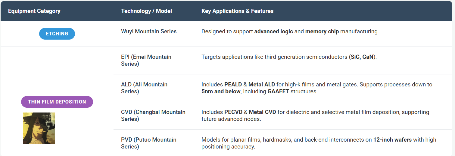
In its initial product launch phase around March 2025, SiCarrier introduced a remarkably broad suite of equipment, all named after famous Chinese mountains, underscoring its comprehensive approach. Etching Equipment, Wuyi Mountain Series, is designed to support advanced logic and memory chip manufacturing. SiCarrier claims these etchers utilize RF/plasma field technology that offers a 10x improvement in energy control precision and hardware response times reduced from 10ms to 1ms, supporting progression to more advanced nodes. The Thin-Film Deposition portfolio is extensive, featuring: EPI equipment under the Emei Mountain Series, targeting applications like third-generation semiconductors (SiC, GaN). ALD equipment, Ali Mountain Series, with products like PEALD and Metal ALD aimed at high-conformality dielectric films and high-aspect-ratio metal gate ALD, reportedly supporting processes down to 5nm and below, including GAAFET structures. CVD equipment, Changbai Mountain Series, including PECVD and Metal CVD for dielectric and selective metal film deposition, also supporting future advanced nodes. PVD equipment, Putuo Mountain Series, with models for metal planar film deposition, mid-process metal contact/hardmask layers, and back-end metal interconnect layers, suitable for 12-inch wafers with high positioning accuracy. SiCarrier has already developed lithography machines capable of processing 300mm wafers for 28nm and older process nodes using DUV technology.
A particularly significant and diverse offering from SiCarrier is in the Metrology and Inspection Equipment category. The BFI (Bright Field patterned Wafer Inspection), Yuelu Mountain Series, utilizes a deep UV broadband plasma light source, large NA objectives, and high-speed detectors for high sensitivity and throughput. The DFI (Dark Field patterned Wafer Inspection), Danxia Mountain Series, employs large NA three-channel collection optics and high-power deep UV continuous lasers. PC (Unpatterned Wafer Surface Inspection, Penglai Mountain Series, using low-noise detectors, high-power deep UV lasers, and high-speed rotary stages. MBI (Mask Blank Inspection), Mogan Mountain Series, features large NA three-channel optics and ultra-clean control. AFM (Atomic Force Microscope), Yimeng Mountain Series, for high-precision surface topography and structure measurement. Additionally, SiCarrier offers Overlay Metrology, Tianmen Mountain Series, including IBO and DBO. X-ray Metrology, Chibi Mountain Series, including XPS, XRD, XRF. Electrical Test Equipment, Lushan Mountain Series, including C-V, IV, and RF Probers. More info here.
SiCarrier is also planning to raise up to $2.8B at a $11B valuation. The proceeds will mostly go towards R&D, and Chinese state-owned firms, state funds, as well as domestic venture capital and private equity funds have expressed interest in investing, said two sources. This unit does not include SiCarrier's lithography assets (crown jewel).

Lithography Equipment (EUV Aspirations)
The lithography equipment segment is one of the most critical and technologically challenging areas in semiconductor manufacturing, currently dominated by a few global players, most notably ASML from the Netherlands, which holds a near-monopoly on EUV (Extreme Ultraviolet) lithography systems essential for advanced nodes below 7nm. Chinese companies are actively working to develop domestic capabilities in lithography, particularly for DUV (Deep Ultraviolet) systems, and have long-term aspirations to enter the EUV space, although this remains a significant challenge. SiCarrier has emerged as a notable domestic contender with ambitious plans. The company reportedly has developed lithography machines capable of processing 300mm wafers for 28nm and older process nodes using DUV technology. Furthermore, SiCarrier has announced a bold roadmap to launch an upgraded version of its lithography equipment by 2026-2027.

SMEE (Shanghai Micro Electronics Equipment Group) is historically China’s leading lithography equipment maker, known to produce machines capable of 28nm technology (SSA800), and is working on more advanced systems. While AMEC is not directly involved in lithography equipment manufacturing, its CEO has expressed the belief that 5nm process nodes might be achievable without EUV, potentially through multipatterning techniques combined with its etching and deposition tools. However, this remains a highly complex and unproven path for volume manufacturing at such advanced nodes. The development of EUV lithography in China faces immense challenges, including the need for high-power EUV light sources, precision optics, high-quality mirrors, and advanced resists, though Chinese entities have filed lots of patents in these areas in the last 2-3 years.
Future Outlook
The Chinese semiconductor equipment industry, spearheaded by companies like AMEC, Naura, ACM Research, Piotech, and the rapidly emerging SiCarrier, is undergoing a period of dynamic growth and ambitious technological advancement. These manufacturers have made significant strides in developing a wide array of critical tools, including etching systems, thin-film deposition (PVD, CVD, ALD) equipment, cleaning solutions, and are venturing into more complex areas like metrology, advanced packaging, and lithography. Their product roadmaps are characterized by aggressive R&D investment, a push towards supporting more advanced process nodes (with some targeting 5-7nm capabilities), and a strong focus on increasing domestic self-sufficiency to reduce reliance on international suppliers. This drive is fueled by both national strategic priorities and the growing demand from China’s expanding semiconductor manufacturing base.
Despite these advancements, Chinese equipment manufacturers still face considerable challenges in matching the breadth, depth, and cutting-edge performance of established global leaders such as ASML, Applied Materials, Lam Research, Tokyo Electron, and KLA. The global leaders benefit from decades of R&D, extensive intellectual property portfolios, deeply entrenched customer relationships, and complex global supply chains that are difficult to replicate quickly. Furthermore, geopolitical factors and export controls continue to pose hurdles for Chinese firms in accessing certain critical technologies and components.

Looking ahead, the future outlook for these Chinese semiconductor equipment manufacturers is one of continued rapid development and increasing competition. The substantial investments being made in R&D and manufacturing capacity are expected to yield further technological breakthroughs and enhance their ability to serve the demands of both domestic and, increasingly, international markets. Key trends to watch include the progress in indigenous lithography, the development of equipment for next-generation transistor architectures (like GAAFETs), and the expansion into advanced packaging technologies. While achieving parity with global leaders across the entire spectrum of semiconductor equipment will be a long-term endeavor, the progress made by these Chinese companies signifies a significant shift in the global semiconductor equipment landscape, promising a more diversified and competitive market in the years to come. Their success will be crucial not only for China’s semiconductor ambitions but also for the overall resilience and evolution of the global semiconductor supply chain.
If u liked my work, then you can support me through BTC- bc1q997zp5mc8r6qke5rqjxcm6amr7wme9er73kdzv, Ethereum- 0xB40279711a7c89A5451ce1A2Db6C66887dBa8d44
This is good shit
Excellent work. Many thanks!